Density Plot of Cation of (BEDT-TTF)2-Cu(NCS)2
The DC program calculates electron density plots for a solid or a layered structure on a crosssection
plane that is parallel to the ab-, ac- or bc-plane of its unit cell. Partial electron density plots are
obtained by using the energy levels belonging to a certain narrow energy region, while total electron
density plots by using all the occupied energy levels. The DP program displays electron density plots
calculated by the DC program. For a layered structure designed to simulate a solid surface, partial and
total electron density plots of interest are "surface density plots" (SDP) calculated on cross-section
planes that are parallel to and lie above the surface at a certain distance.
Atomic- and molecular-scale STM and AFM images are almost routinely recorded for crystalline surfaces, but the interpretation of these images is not necessarily straightforward because the tip-sample force interaction may induce a surface corrugation, which depends on the variation of the local stiffness of the sample surface. If the tip-force induced surface corrugation is neglected, an STM image of a sample surface recorded with positive bias voltage is described by a partial SDP associated with the lowest unoccupied energy levels of the sample surface, and an STM image recorded with negative bias voltage by a partial SDP associated with the highest occupied energy levels. An AFM image of a sample surface is described by the total SDP resulting from all the occupied energy levels of the sample surface.
Atomic- and molecular-scale STM and AFM images are almost routinely recorded for crystalline surfaces, but the interpretation of these images is not necessarily straightforward because the tip-sample force interaction may induce a surface corrugation, which depends on the variation of the local stiffness of the sample surface. If the tip-force induced surface corrugation is neglected, an STM image of a sample surface recorded with positive bias voltage is described by a partial SDP associated with the lowest unoccupied energy levels of the sample surface, and an STM image recorded with negative bias voltage by a partial SDP associated with the highest occupied energy levels. An AFM image of a sample surface is described by the total SDP resulting from all the occupied energy levels of the sample surface.
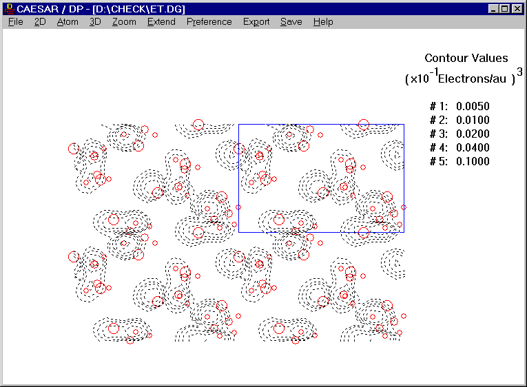
Figure. Density Plot of Cation of (BEDT-TTF)2-Cu(NCS)2